1. Material Fundamentals and Architectural Features of Alumina Ceramics
1.1 Crystallographic and Compositional Basis of α-Alumina
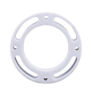
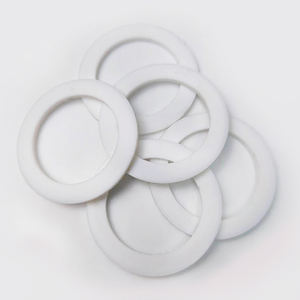
(Alumina Ceramic Substrates)
Alumina ceramic substratums, primarily made up of aluminum oxide (Al ₂ O ₃), work as the foundation of modern-day electronic packaging as a result of their outstanding equilibrium of electric insulation, thermal stability, mechanical toughness, and manufacturability.
The most thermodynamically secure phase of alumina at heats is diamond, or α-Al ₂ O FIVE, which takes shape in a hexagonal close-packed oxygen lattice with aluminum ions occupying two-thirds of the octahedral interstitial websites.
This dense atomic arrangement conveys high solidity (Mohs 9), excellent wear resistance, and solid chemical inertness, making α-alumina ideal for rough operating environments.
Industrial substrates typically include 90– 99.8% Al Two O THREE, with small additions of silica (SiO ₂), magnesia (MgO), or rare earth oxides utilized as sintering help to promote densification and control grain development throughout high-temperature handling.
Greater pureness grades (e.g., 99.5% and above) display remarkable electrical resistivity and thermal conductivity, while reduced purity variants (90– 96%) use cost-efficient services for much less demanding applications.
1.2 Microstructure and Flaw Engineering for Electronic Reliability
The performance of alumina substratums in electronic systems is critically dependent on microstructural uniformity and flaw minimization.
A penalty, equiaxed grain structure– generally ranging from 1 to 10 micrometers– makes certain mechanical integrity and decreases the chance of fracture proliferation under thermal or mechanical tension.
Porosity, particularly interconnected or surface-connected pores, need to be lessened as it degrades both mechanical toughness and dielectric performance.
Advanced handling methods such as tape spreading, isostatic pushing, and controlled sintering in air or regulated ambiences enable the manufacturing of substrates with near-theoretical thickness (> 99.5%) and surface roughness below 0.5 µm, necessary for thin-film metallization and wire bonding.
Furthermore, pollutant partition at grain boundaries can result in leakage currents or electrochemical movement under prejudice, demanding rigorous control over resources purity and sintering conditions to ensure long-term dependability in damp or high-voltage environments.
2. Production Processes and Substratum Fabrication Technologies
( Alumina Ceramic Substrates)
2.1 Tape Casting and Environment-friendly Body Processing
The manufacturing of alumina ceramic substratums begins with the preparation of an extremely dispersed slurry including submicron Al two O ₃ powder, organic binders, plasticizers, dispersants, and solvents.
This slurry is processed by means of tape spreading– a continuous technique where the suspension is spread over a relocating service provider movie utilizing a precision doctor blade to attain consistent density, usually between 0.1 mm and 1.0 mm.
After solvent dissipation, the resulting “eco-friendly tape” is flexible and can be punched, drilled, or laser-cut to form using openings for upright affiliations.
Multiple layers may be laminated to produce multilayer substrates for intricate circuit integration, although the majority of commercial applications utilize single-layer setups due to set you back and thermal growth factors to consider.
The environment-friendly tapes are then thoroughly debound to eliminate organic additives via regulated thermal decay prior to last sintering.
2.2 Sintering and Metallization for Circuit Integration
Sintering is carried out in air at temperature levels between 1550 ° C and 1650 ° C, where solid-state diffusion drives pore elimination and grain coarsening to attain complete densification.
The direct shrinkage during sintering– typically 15– 20%– need to be specifically predicted and made up for in the layout of eco-friendly tapes to make sure dimensional precision of the final substratum.
Adhering to sintering, metallization is put on create conductive traces, pads, and vias.
Two primary methods control: thick-film printing and thin-film deposition.
In thick-film innovation, pastes including steel powders (e.g., tungsten, molybdenum, or silver-palladium alloys) are screen-printed onto the substratum and co-fired in a reducing environment to form robust, high-adhesion conductors.
For high-density or high-frequency applications, thin-film procedures such as sputtering or evaporation are made use of to deposit adhesion layers (e.g., titanium or chromium) complied with by copper or gold, enabling sub-micron patterning through photolithography.
Vias are loaded with conductive pastes and terminated to develop electrical affiliations between layers in multilayer styles.
3. Useful Features and Performance Metrics in Electronic Equipment
3.1 Thermal and Electrical Behavior Under Operational Anxiety
Alumina substrates are prized for their positive combination of modest thermal conductivity (20– 35 W/m · K for 96– 99.8% Al Two O FOUR), which allows reliable heat dissipation from power tools, and high volume resistivity (> 10 ¹⁴ Ω · centimeters), ensuring marginal leak current.
Their dielectric consistent (εᵣ ≈ 9– 10 at 1 MHz) is stable over a wide temperature and regularity variety, making them appropriate for high-frequency circuits as much as a number of ghzs, although lower-κ products like light weight aluminum nitride are favored for mm-wave applications.
The coefficient of thermal growth (CTE) of alumina (~ 6.8– 7.2 ppm/K) is reasonably well-matched to that of silicon (~ 3 ppm/K) and certain product packaging alloys, lowering thermo-mechanical anxiety throughout tool operation and thermal cycling.
However, the CTE inequality with silicon continues to be an issue in flip-chip and direct die-attach setups, frequently requiring certified interposers or underfill materials to minimize fatigue failure.
3.2 Mechanical Toughness and Ecological Toughness
Mechanically, alumina substrates exhibit high flexural toughness (300– 400 MPa) and excellent dimensional security under lots, allowing their usage in ruggedized electronic devices for aerospace, automotive, and commercial control systems.
They are immune to resonance, shock, and creep at elevated temperatures, preserving architectural honesty as much as 1500 ° C in inert environments.
In moist environments, high-purity alumina shows minimal moisture absorption and superb resistance to ion movement, making sure lasting reliability in outdoor and high-humidity applications.
Surface area firmness likewise safeguards versus mechanical damage during handling and setting up, although care needs to be required to prevent side chipping as a result of fundamental brittleness.
4. Industrial Applications and Technological Influence Across Sectors
4.1 Power Electronics, RF Modules, and Automotive Equipments
Alumina ceramic substratums are common in power electronic components, including protected entrance bipolar transistors (IGBTs), MOSFETs, and rectifiers, where they supply electrical isolation while facilitating heat transfer to warmth sinks.
In radio frequency (RF) and microwave circuits, they function as provider platforms for crossbreed incorporated circuits (HICs), surface acoustic wave (SAW) filters, and antenna feed networks due to their secure dielectric residential or commercial properties and low loss tangent.
In the automobile sector, alumina substrates are used in engine control units (ECUs), sensor packages, and electrical vehicle (EV) power converters, where they withstand high temperatures, thermal cycling, and exposure to destructive liquids.
Their integrity under harsh problems makes them vital for safety-critical systems such as anti-lock stopping (ABDOMINAL) and advanced vehicle driver aid systems (ADAS).
4.2 Medical Devices, Aerospace, and Arising Micro-Electro-Mechanical Equipments
Beyond customer and industrial electronics, alumina substratums are utilized in implantable clinical tools such as pacemakers and neurostimulators, where hermetic sealing and biocompatibility are critical.
In aerospace and defense, they are utilized in avionics, radar systems, and satellite communication modules due to their radiation resistance and security in vacuum environments.
Moreover, alumina is increasingly used as a structural and insulating system in micro-electro-mechanical systems (MEMS), including pressure sensors, accelerometers, and microfluidic gadgets, where its chemical inertness and compatibility with thin-film handling are beneficial.
As digital systems continue to demand greater power thickness, miniaturization, and dependability under extreme problems, alumina ceramic substratums stay a keystone material, connecting the void in between performance, price, and manufacturability in sophisticated electronic product packaging.
5. Supplier
Alumina Technology Co., Ltd focus on the research and development, production and sales of aluminum oxide powder, aluminum oxide products, aluminum oxide crucible, etc., serving the electronics, ceramics, chemical and other industries. Since its establishment in 2005, the company has been committed to providing customers with the best products and services. If you are looking for high quality mcdanel alumina, please feel free to contact us. (nanotrun@yahoo.com)
Tags: Alumina Ceramic Substrates, Alumina Ceramics, alumina
All articles and pictures are from the Internet. If there are any copyright issues, please contact us in time to delete.
Inquiry us