1. Fundamental Residences and Nanoscale Habits of Silicon at the Submicron Frontier
1.1 Quantum Confinement and Electronic Structure Improvement
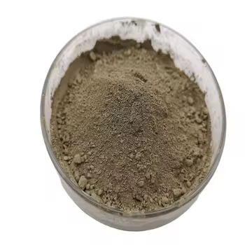
(Nano-Silicon Powder)
Nano-silicon powder, made up of silicon bits with particular dimensions below 100 nanometers, represents a paradigm shift from bulk silicon in both physical behavior and useful utility.
While mass silicon is an indirect bandgap semiconductor with a bandgap of roughly 1.12 eV, nano-sizing causes quantum arrest impacts that fundamentally modify its electronic and optical residential or commercial properties.
When the bit size techniques or falls listed below the exciton Bohr span of silicon (~ 5 nm), fee carriers end up being spatially confined, leading to a widening of the bandgap and the appearance of visible photoluminescence– a sensation missing in macroscopic silicon.
This size-dependent tunability enables nano-silicon to give off light across the visible spectrum, making it an appealing prospect for silicon-based optoelectronics, where traditional silicon falls short because of its poor radiative recombination efficiency.
Moreover, the increased surface-to-volume ratio at the nanoscale improves surface-related sensations, including chemical reactivity, catalytic task, and communication with magnetic fields.
These quantum effects are not simply scholastic inquisitiveness however form the structure for next-generation applications in energy, picking up, and biomedicine.
1.2 Morphological Diversity and Surface Chemistry
Nano-silicon powder can be synthesized in different morphologies, including spherical nanoparticles, nanowires, permeable nanostructures, and crystalline quantum dots, each offering unique advantages depending on the target application.
Crystalline nano-silicon generally keeps the ruby cubic structure of mass silicon yet exhibits a greater thickness of surface area flaws and dangling bonds, which should be passivated to support the product.
Surface area functionalization– often attained with oxidation, hydrosilylation, or ligand attachment– plays a crucial role in establishing colloidal security, dispersibility, and compatibility with matrices in compounds or organic environments.
For example, hydrogen-terminated nano-silicon shows high reactivity and is vulnerable to oxidation in air, whereas alkyl- or polyethylene glycol (PEG)-covered particles exhibit improved security and biocompatibility for biomedical use.
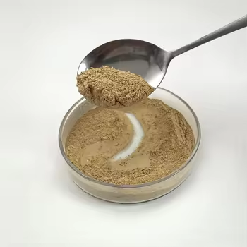
( Nano-Silicon Powder)
The visibility of an indigenous oxide layer (SiOₓ) on the bit surface area, also in minimal quantities, substantially affects electrical conductivity, lithium-ion diffusion kinetics, and interfacial responses, especially in battery applications.
Comprehending and regulating surface area chemistry is consequently necessary for taking advantage of the complete potential of nano-silicon in sensible systems.
2. Synthesis Strategies and Scalable Construction Techniques
2.1 Top-Down Strategies: Milling, Etching, and Laser Ablation
The manufacturing of nano-silicon powder can be broadly classified right into top-down and bottom-up approaches, each with distinctive scalability, pureness, and morphological control characteristics.
Top-down methods entail the physical or chemical decrease of bulk silicon right into nanoscale pieces.
High-energy sphere milling is a widely made use of industrial method, where silicon portions go through extreme mechanical grinding in inert ambiences, resulting in micron- to nano-sized powders.
While cost-efficient and scalable, this approach often presents crystal defects, contamination from grating media, and wide fragment dimension distributions, needing post-processing filtration.
Magnesiothermic decrease of silica (SiO ₂) adhered to by acid leaching is one more scalable course, especially when utilizing all-natural or waste-derived silica resources such as rice husks or diatoms, supplying a lasting pathway to nano-silicon.
Laser ablation and reactive plasma etching are extra accurate top-down methods, capable of creating high-purity nano-silicon with regulated crystallinity, however at greater cost and lower throughput.
2.2 Bottom-Up Approaches: Gas-Phase and Solution-Phase Growth
Bottom-up synthesis permits higher control over particle size, form, and crystallinity by constructing nanostructures atom by atom.
Chemical vapor deposition (CVD) and plasma-enhanced CVD (PECVD) allow the development of nano-silicon from gaseous forerunners such as silane (SiH ₄) or disilane (Si ₂ H SIX), with specifications like temperature, stress, and gas circulation determining nucleation and development kinetics.
These techniques are particularly effective for generating silicon nanocrystals embedded in dielectric matrices for optoelectronic devices.
Solution-phase synthesis, consisting of colloidal paths utilizing organosilicon substances, enables the production of monodisperse silicon quantum dots with tunable discharge wavelengths.
Thermal disintegration of silane in high-boiling solvents or supercritical fluid synthesis additionally generates top notch nano-silicon with slim size distributions, appropriate for biomedical labeling and imaging.
While bottom-up methods usually create remarkable material top quality, they face difficulties in large production and cost-efficiency, requiring recurring study into hybrid and continuous-flow processes.
3. Energy Applications: Reinventing Lithium-Ion and Beyond-Lithium Batteries
3.1 Duty in High-Capacity Anodes for Lithium-Ion Batteries
Among the most transformative applications of nano-silicon powder depends on power storage, particularly as an anode material in lithium-ion batteries (LIBs).
Silicon uses an academic particular capacity of ~ 3579 mAh/g based upon the development of Li ₁₅ Si Four, which is nearly 10 times higher than that of traditional graphite (372 mAh/g).
However, the large quantity growth (~ 300%) during lithiation causes bit pulverization, loss of electrical contact, and constant solid electrolyte interphase (SEI) formation, leading to fast capability fade.
Nanostructuring reduces these issues by reducing lithium diffusion paths, fitting pressure better, and reducing crack possibility.
Nano-silicon in the type of nanoparticles, permeable structures, or yolk-shell structures makes it possible for reversible cycling with enhanced Coulombic efficiency and cycle life.
Industrial battery modern technologies now integrate nano-silicon blends (e.g., silicon-carbon compounds) in anodes to increase energy density in customer electronics, electric cars, and grid storage systems.
3.2 Potential in Sodium-Ion, Potassium-Ion, and Solid-State Batteries
Past lithium-ion systems, nano-silicon is being discovered in emerging battery chemistries.
While silicon is much less responsive with salt than lithium, nano-sizing enhances kinetics and allows minimal Na ⁺ insertion, making it a candidate for sodium-ion battery anodes, particularly when alloyed or composited with tin or antimony.
In solid-state batteries, where mechanical security at electrode-electrolyte user interfaces is vital, nano-silicon’s capability to go through plastic contortion at small ranges reduces interfacial tension and enhances get in touch with maintenance.
In addition, its compatibility with sulfide- and oxide-based solid electrolytes opens up opportunities for much safer, higher-energy-density storage options.
Study remains to enhance interface design and prelithiation methods to make the most of the durability and efficiency of nano-silicon-based electrodes.
4. Emerging Frontiers in Photonics, Biomedicine, and Composite Products
4.1 Applications in Optoelectronics and Quantum Source Of Light
The photoluminescent homes of nano-silicon have revitalized efforts to develop silicon-based light-emitting gadgets, a long-lasting challenge in integrated photonics.
Unlike bulk silicon, nano-silicon quantum dots can exhibit reliable, tunable photoluminescence in the visible to near-infrared array, allowing on-chip lights suitable with complementary metal-oxide-semiconductor (CMOS) innovation.
These nanomaterials are being incorporated into light-emitting diodes (LEDs), photodetectors, and waveguide-coupled emitters for optical interconnects and noticing applications.
Furthermore, surface-engineered nano-silicon shows single-photon discharge under certain problem configurations, placing it as a potential platform for quantum information processing and secure communication.
4.2 Biomedical and Ecological Applications
In biomedicine, nano-silicon powder is gaining interest as a biocompatible, naturally degradable, and safe option to heavy-metal-based quantum dots for bioimaging and medicine distribution.
Surface-functionalized nano-silicon fragments can be made to target details cells, launch restorative agents in action to pH or enzymes, and supply real-time fluorescence tracking.
Their degradation into silicic acid (Si(OH)FOUR), a normally occurring and excretable compound, reduces long-lasting toxicity problems.
Furthermore, nano-silicon is being checked out for ecological remediation, such as photocatalytic destruction of toxins under visible light or as a lowering representative in water therapy processes.
In composite products, nano-silicon enhances mechanical strength, thermal stability, and wear resistance when included into steels, porcelains, or polymers, particularly in aerospace and automotive parts.
In conclusion, nano-silicon powder stands at the intersection of essential nanoscience and commercial advancement.
Its unique mix of quantum impacts, high reactivity, and convenience across energy, electronic devices, and life sciences highlights its function as a vital enabler of next-generation technologies.
As synthesis techniques development and assimilation challenges relapse, nano-silicon will certainly continue to drive progression toward higher-performance, sustainable, and multifunctional product systems.
5. Vendor
TRUNNANO is a supplier of Spherical Tungsten Powder with over 12 years of experience in nano-building energy conservation and nanotechnology development. It accepts payment via Credit Card, T/T, West Union and Paypal. Trunnano will ship the goods to customers overseas through FedEx, DHL, by air, or by sea. If you want to know more about Spherical Tungsten Powder, please feel free to contact us and send an inquiry(sales5@nanotrun.com).
Tags: Nano-Silicon Powder, Silicon Powder, Silicon
All articles and pictures are from the Internet. If there are any copyright issues, please contact us in time to delete.
Inquiry us